


Please Leave Us A Message
Privacy statement: Your privacy is very important to Us. Our company promises not to disclose your personal information to any external company with out your explicit permission.
 March 31, 2023
High-power LEDs are favored by people for their high efficiency, pollution-free, long life and many other advantages. However, high-power LEDs require low-voltage, high-current driving power supplies. In order to highlight the advantages of high-power LEDs, it is required to have a driving power supply. Higher efficiency, higher power factor, and overvoltage, overcurrent, and overtemperature protection.
1 Principle and design
The circuit designed in this paper is mainly divided into three parts: EMI module, PFC converter and DC/DC Converter. The EMI module adopts double-loop filtering to achieve better results. The Fairchild FAN6961 chip is used as the control chip of PFC converter. The Boost transform is used to improve the power factor. The DC/DC converter uses LLC resonance and uses FSFR2100 as the control device to achieve high efficiency. The basic structure is shown in Figure 1.
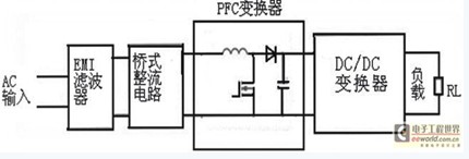
Figure 1 drive power design structure
1.1 EMI Module
The interference signal of the switching power supply can be divided into a common mode interference signal and a differential mode interference signal according to the conduction mode. The characteristics can be roughly divided into three frequency bands:
0.15~0.5MHz differential mode interference is dominant; 0.5~5MHz difference, common mode interference coexist; 5~30MHz common mode interference is dominant. At the time of design, if any frequency band is not up to standard, the filtering effect can be enhanced for this frequency band. For example, in the 0.15~0.5MHz frequency band, the suppression of the differential mode interference signal can be enhanced, the value of the capacitance Cx can be increased or the differential mode choke coil can be added; if the frequency range is not reached in the 5~30MHz frequency band, the suppression of the common mode interference signal can be enhanced. Increase the value of Cy or increase the number of stages of common mode filtering. When suppressing interference signals, the focus is on the suppression of common mode interference signals.

1.2 PFC converter design
1.2.1 How Boost Transformation Works
Boost converters are also known as parallel switching converters. When the control signal is turned on to turn on the switching transistor VT, energy is input from the input power source and stored in the inductor L. The diode VD is reverse biased, and the load is supplied by the filter capacitor C.
When VT is turned off, the current in the inductor L cannot be abruptly changed, and the induced potential generated by it prevents the current from decreasing, and the polarity of the potential is left-right and right-right. The diode VD is turned on, and the energy stored in the inductor flows into the capacitor C through the diode VD and is supplied to the load.
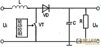
Figure 3 Boost converter circuit structure
1.2.2 Boost-based PFC converter design
We can see that during the conduction of the switch, the inductor voltage is equal to the input voltage, the inductor current increases linearly, the diode D1 is cut off, the voltage of the auxiliary winding increases, and the voltage of the current sense resistor rises linearly; when the on-time reaches Ton When the switch is disconnected. When the switch tube is disconnected, the inductor voltage is reduced, the inductor current flows to the load through the diode D1, the voltage of the auxiliary winding is reduced, and no current flows through the current detecting resistor. Before the switch tube is turned on again, the voltage on the current detecting resistor is already 0. The voltage waveform of the zero current detection terminal is exactly opposite to the pulse of the drive waveform of the switch tube. When the voltage of the zero current detection terminal will be 0, the switch tube starts to conduct again, and a new cycle begins. It can be seen that the circuit operates in a critical conduction mode.
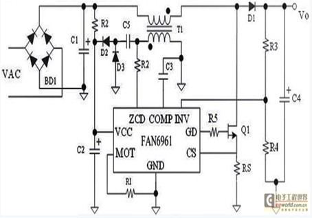
Figure 4 FAN6961 peripheral circuit
From the following equation, we find that the current stress of the switch S is: 1.93A.

Formula 1
Since the PFC stage output voltage range is 400 ± 20V, V0_max = 420V, consider selecting the PDPF20N50 switching transistor (VDS=500V, ID=12.9A, RDS(on)=0.2Ω).
In order to reduce noise, the switching frequency of the Boost converter should be as low as possible, but it must be greater than 20 kHz (below the 20 kHz human ear can hear). In this study, fmin=40 kHz is set. At this time, the effective value of the input voltage is VRMS=265V, Vin=√2VRMS=374V, V0=400V, and the input power Pin=P0/η=150/0.85=176.5W. Substituting the following formula: L = 220H.
 Equation 2
Select the inductor L=220H, select PQ3230 as the core, and check the parameters of each parameter. The effective area of the core is Ae=161mm2, AL=5140nH/N2, Le=7.46cm, and the highest working magnetic density of the core is Bs=0.32T. The peak induced current of the inductor:
 Equation 3
The number of turns of the inductor is determined by equation (4):
 Equation 4
Round up the result of the above formula and set the number of turns to 26.
The control chip of the Boost converter is FAN6961, which requires an auxiliary winding. According to the instructions of FAN6961, the number of turns is determined by equation (5):
 Equation 5
For the above formula, the number of turns of the auxiliary winding is 3.
In the PFC circuit, a small capacitor is usually connected to the output end of the rectifier bridge, which is mainly used for filtering high frequency noise at the input end, and its capacity is generally small. Its value has a lower limit value and an upper limit value, and the lower limit value is determined by the maximum voltage ripple of the input filter capacitor, and the upper limit value is determined by the offset angle between the input current and the input voltage.
Vin(min)=√2Vin_RMS_min=120V, according to the reference, ΔVci(max) generally takes 5% of the minimum input voltage peak. ΔVci(max)=5%Vin(min)=6V, L=220H, Pin=P0/η=150/0.85=176.5W, V0=400V, cosβ=0.9, ω=100π. Substitute into the following formula:
 Equation 6
 Equation 7
From the above formula, Cin min=0.67μF and Cin max=3.89μF. In this paper, the input capacitor is 684/630V.
Vmax=ΔVci(max)/2=3V, f=50Hz, f=50Hz, I0=P0/V0=0.375A are substituted into the following formula:
 Equation 8
Obtained: C0 min=199μF, considering that the maximum output voltage is 420V, in this experiment, an electrolytic capacitor with a capacity of 220 and a withstand voltage of 450V is selected.
1.3 DC / DC converter design
1.3.1 DC/DC converter based on LLC resonance
The LLC resonant converter is superior to conventional series resonant converters and parallel resonant converters. First, it can adjust the output with a wide range of input and load changes, while the switching frequency changes relatively little. Second, it achieves zero voltage switching (ZVS) over the entire operating range, reducing switching losses and increasing efficiency. Finally, all parasitic components, including the junction capacitance of all semiconductor devices and the leakage inductance and magnetizing inductance of the transformer, are used to implement ZVS.
Figure 5 shows the working principle of an LLC resonant converter. The LLC resonant converter typically includes a controller with a MOSFET (this article uses FSFR2100 as the controller), a resonant network, and a rectification network.

Figure 5 LLC resonant converter working principle diagram
The FSFR2100 alternately drives two MOSFETs with a 50% duty cycle, changing the operating frequency as the load changes, and adjusting the output voltage. The resonant network includes two resonant inductors and one resonant capacitor. The resonant inductors Ls, Lm and the resonant capacitor Cs act primarily as a voltage divider whose impedance varies with the operating frequency to achieve the desired output voltage. The rectifying network rectifies the sinusoidal waveform generated by the resonant network and transmits it to the output stage.
1.3.2 Calculation of various parameters of LLC resonance
Minimum voltage gain by formula  Where K is 8, the minimum voltage gain is:
 Equation 9
As shown in Figure 6.

Figure 6 Minimum voltage gain
Know the PFC stage output voltage is  =405V, after finding the transformer output terminal rectifier diode FFPF12UP2ODN voltage drop VF=1.15V, the output voltage V0=50V is required, the transformer turns ratio n is:
 Equation 10
For the same specification, the resonant inductor and the capacitor can take different values. Here, the value of Cr has a lower limit. The value of Cr needs to make the series resonant tank work in a constant gain interval, and selecting a larger Cr will make The voltage stress on Cr is lowered. The problem with this is that the impedance of the resonant tank is lowered, which affects the performance at the time of short circuit. When the impedance of the resonant tank is lowered, the current is increased at the time of the short circuit, and in order to limit the short-circuit current, a higher switching frequency is required. Here, a capacitor of 22nF withstand voltage of 630V is selected.
By formula  Deduced:
 Equation 11

Figure 7 Typical gain curve of a LLC resonant converter (k=8)
As shown in the typical voltage gain curve of the oscillator of Figure 7, the resonant frequency is chosen to be 102 kHz, and in the previous step, Cr = 22 nF has been obtained. Substituting these two parameters into equation (11) gives:
 Equation 12
Substituting k=8, Lr=110μH into equation (13):
 Equation 13
Get:
 Equation 14
The core of the transformer is selected as EER3542 (Ae=107mm2) core. The minimum switching frequency is 77kHz from the gain curve shown in Figure 7. The minimum number of primary coils of the transformer is:
 Equation 15
When the number of turns of the secondary coil is 8, the number of turns of the primary coil is established, so the number of turns of the transformer is: primary NP=36Ts, secondary Ns=8Ts.
2 Conclusion
The high-Power LED Driver circuit designed in this paper uses fewer components, and the circuit is simple. The FAN6961 chip is used to combine the Boost circuit and the PFC module, and the LLC resonant converter is used to achieve higher efficiency. The higher power factor greatly reduces electromagnetic interference, which is safe and reliable.
Edit: Sophy
The above is the Research and design of high power LED driver circuit we have listed for you. You can submit the following form to obtain more industry information we provide for you.
You can visit our website or contact us, and we will provide the latest consultation and solutions
Send Inquiry
Most Popular
lastest New
Send Inquiry

Privacy statement: Your privacy is very important to Us. Our company promises not to disclose your personal information to any external company with out your explicit permission.
Fill in more information so that we can get in touch with you faster
Privacy statement: Your privacy is very important to Us. Our company promises not to disclose your personal information to any external company with out your explicit permission.